Pushing Pixels
This post is the second in a series looking at the design and implementation of my Glitch demo and the m4vgalib code that powers it.
Updated 2015-06-10: clarifications from reader feedback.
For the first technical part in the series, I’d like to start from the very end: getting the finished pixels out of the microprocessor and off to a display.
Why start from the end? Because it’s where I started in my initial experiments, and because my decisions here had significant effects on the shape of the rest of the system.
Intro to analog video and VGA
The standard we call “VGA” isn’t really called VGA1, and isn’t much of a standard2. But it has no good name other than VGA, so I’ll stick with that.
“VGA” is actually the name of the IBM hardware that first produced this style of video. Nobody but collectors has these anymore.
It’s actually a bag of dozens of slightly incompatible standards, which the public cannot read without paying money. Good times.
I’ll go into more detail about VGA as we need it in future posts, but here’s the short version, filled with Wikipedia links if you want to read ahead:
VGA is an analog video standard that uses component video with separate sync signals. Like most analog video standards, it’s distantly related to analog television signals, which are themselves an electrical relative of the mechanical televisions of the late 19th century. Seriously, people built mechanical televisions. Steampunk, eat your heart out.
Anyway. VGA dominated the industry from 1987 up until about 2005, and is still ubiquitous — I bet you can find at least one device in your household with a VGA input or output. (Try the back of your television.)
Generating stable, high-quality VGA video at high resolutions is a complicated topic — I should know, I’ve been working on it for three years — but for today’s post, only one part matters: the pixel clock.
A VGA monitor expects to receive pixels — more precisely, it expects to receive changes in three voltages, one each for red, green, and blue. Each voltage corresponds (hence “analog”) to the intensity of the corresponding color component. The signals are just electrical waves, without any way of indicating the boundaries between pixels. Instead, the circuit producing the video (us!) and the one receiving it (a display) perform an intricate timing dance to agree on a pixel clock — an implicit but shared “beat” that indicates when the voltages represent one pixel, and when they change to describing the next.
It’s really easy to get this wrong, even in professional video hardware. If you’ve ever plugged a computer into a display to get fuzzy output, only to unplug and plug it in again and have things come out sharp, you’ve seen the timing dance fail and recover. This is why VGA monitors have an “autosync” feature or button to retry the dance.
So we need to put effort into getting this right, and it all starts with producing pixels at one of the standard rates.
In our case, the target is the VESA 800x600 60fps non-interlaced mode, for which we need to produce pixels at a very precise 40MHz rate — or one pixel every 25 nanoseconds. Shifting the signal by even five nanoseconds in either direction would visibly mar our beautiful video! We’re going to have to be careful.
Now let’s turn to the hardware we’re using.
About the STM32F407
The STM32F407 is a microcontroller from ST Microsystems, based around the popular ARM Cortex-M4F core. In terms of compute power, instruction latency, and overall capabilities, it is very much like a late-generation 486, only slightly faster and from a bizarro world where the 486 was RISC. So if you’re reading Abrash’s book — and you should — stop before the Pentium section3.
Unless you want a preview of the sorts of tricks you’ll need to wring every last drop of performance from a Cortex-M7, which is curiously similar to an early Pentium. The more things change, the more things change the same.
The STM32F407 variant I’m using has 192 kiB of RAM and 512 kiB of Flash, which is roughly the amount of storage available in, say, an unexpanded Commodore 128 or the original Macintosh. But those computers have something I don’t: hardware for producing video. While the ’407 also has a whole mess of interesting peripherals, video generation is not among them4. Which is, of course, why we’re here!
The STM32F427 and friends were paper-launched before I started this project, but shipped well after. They have LCD controllers. Yes, you can trick their LCD controller into doing 800x600. No, that does not sound like an interesting problem to me. ;-)
The peripherals it does have are documented at length — albeit at varying levels of quality — in the Reference Manual.
Did I mention the Reference Manual?
No, really, if you want to follow along with the really fun stuff, stash a copy of the Reference Manual. While it’s not perfect, it’s important, and I will refer back to it.
Note: Unfortunately, STMicro renumbers sections and figures willy-nilly between editions of the manual, making it damn hard to refer conclusively to anything in there. Where I need to cite the manual I will give the section/figure/table number in my copy, plus any titles or captions to help you track it down in yours. Please send me corrections if STMicro changes everything again. :-(
Let me draw your attention to two particular items in the Reference Manual. The first is so important that I’m going to reproduce it outright, without permission5. Behold, the almighty powerful, and almighty cryptic, Figure 1:
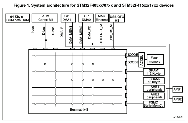
I’m pretty confident my use of this image in this and subsequent articles is fair use, but STMicro, before getting mad, please consider that I am essentially writing a multi-part advertisement for your chips, while taking only the occasional potshot at your beleaguered tech writers.
This is the AHB bus matrix diagram for the STM32F407 and related chips. It is not just a pretty face: it’s the key to unlocking the full performance of this chip.
Second, there is Table 1, or STM32F4xx register boundary addresses. In my copy of the Manual it’s in section 2.3, “Memory Map.” This table tells you, for every peripheral on the chip, which exit from Figure 1’s AHB Matrix to use to access it. As a normal programmer you’d rarely need this information — but if you’re still reading, you are either an abnormal programmer, or soon will be.
Getting pixels out
We need a way of making three analog signals — red, green, and blue — produce around 40 million samples per second (MS/s). A quick skim of the Reference Manual shows that the STM32F407 has a bazillion peripherals of various kinds; how many of them are relevant here?
None of the analog output peripherals, that’s for certain: there are only two DAC channels, and they top out at just 1 MS/s6. So we’ll have to produce digital output and convert it to analog voltages outside the chip.
If you had a hard time finding this number in the Reference Manual, that’s because it isn’t in there. It’s in the part-specific datasheet, even though it’s the same for every STM32F4 part. Hooray STMicro.
We need n parallel output bits to display 2^n^ colors. 256 colors seemed like a reasonable place to start, but I kept an eye out for anything that would let me do 16-bit (65,536 colors on screen). Two peripherals seemed to fit the bill:
- The “Flexible Static Memory Controller,” or FSMC.
- The GPIO ports.
On previous video projects I had used things like SPI controllers to generate monochrome video. While this sticks you with monochrome, it has a big advantage: these controllers often have built-in FIFOs, or at the very least a wide shift register. This lets you compute a few pixels’ worth of the image (often 32), stuff it into the FIFO, and go off and do other things, freed (for now) of your real-time obligations to the display.
On the STM32F4, neither the FSMC nor the GPIO have FIFOs7. But that’s okay, because also featured in the Reference Manual is the General Purpose DMA Controller. We can use DMA to set up flows of data between memory and any peripheral, including FSMC and GPIO.
In fact, weirdly few of the STM32F4 peripherals have FIFOs. Particularly surprising: the UARTs don’t have receive FIFOs, which makes it tricky to achieve high bit rates. You basically have to use DMA.
So which one’s better? The answer surprised me. But first, an aside on the pecularities of the STM32F4 DMA controller.
A quick DMA refresher
In case you haven’t used DMA before, a DMA controller is sort of like a really simple second processor that can be programmed to do a single thing: copy bytes from one address to another. It can do this without hassling the main processor for help, hence direct memory access. The STM32F4’s DMA controller is relatively fancy, as these things go, but still pretty simple.
DMA is mediated by DMA Requests, or DRQs. They’re like IRQs for the main processor, but they trigger behavior in the DMA controller instead. In the case of the STM32F4, each DRQ can trigger a single “transfer,” which is a copy of a (small) configurable number of bytes from one place to another.
When you program the DMA controller to do your bidding, you set a “number of data items” counter. Every time a DRQ happens, the DMA controller decrements it8. When it reaches zero, the transfer is marked “complete” and further DRQs are ignored until it’s turned back on.
In case there are any truly pedantic STM32F4 experts in the audience, I will acknowledge that there’s one case where what I said is not true: when using DMA with the SDIO controller you can use a “peripheral flow controller” mode, where the peripheral decides how much data to transfer. I assert that it isn’t a generally useful feature, which is why it appears only in a footnote.
I remember DMA controllers being pretty intimidating when I first started doing embedded programming, but they’re not hard — just a little tedious. They are now my bestest friend, to the point that I just don’t reach for processors without good general DMA controllers anymore.
DMA on STM32F4 (or: when is direct memory access not direct?)
To blow some data out a port (GPIO or FSMC) under DMA control on an STM32F4, the basic procedure looks something like this:
-
Turn on the DMA controller and your peripheral9.
9I have totally never lost an evening to forgetting to do this. Nope, no sir.
-
Pick a DMA Stream to use.
-
Arrange to have its associated DRQ strummed periodically.
-
Turn it on.
-
Kick back.
Simple! And this is where things get tedious, with a good bit of Reference Manual cross-referencing. :-)
First, pick which DMA stream you want to use. There are 16 such streams, 8 on each of two DMA controllers. Each of the 16 streams can have its own transfer ongoing, independent of the others. However, you can’t pick just any stream.
If you refer to the almighty Figure 1 again, you’ll notice the two DMA controllers at the top. Each has two ports emerging from its underside; ST calls these ports the “memory” and “peripheral” ports, and they are bus masters.
The big block in the middle of Figure 1 is the AHB Bus Matrix. I’ll take a closer look at the matrix in a future installment. The key for now: nothing, the CPU included10, really has direct access to memory. It’s all intermediated by the bus matrix.
Okay, technically, the CPU does have direct access to the 64kiB Closely Coupled Memory, or CCM — with the effect that it isn’t available for DMA!
But note that GPDMA1’s peripheral port doesn’t actually connect to the bus matrix. Instead, it runs off to the right, bypassing the matrix and connecting directly to APB1. This means that, while GPDMA1’s “memory” side can talk to all sorts of memory, GPDMA1’s peripheral side can only talk to peripherals on the APB1 bus.
Which is bad, because — according to Table 1 — none of the peripherals we’re discussing live on APB1.
GPDMA2’s peripheral port also has a line running off to the right (eventually ending up in APB2), but that line forks, and also joins the AHB matrix fabric as a master. So GPDMA2’s peripheral port is more general than GPDMA1’s: it can talk to a variety of things through the matrix, including peripherals that live directly on AHB instead of APB.
Since (per Table 1) the GPIO lives on AHB1 and the FSMC on AHB3, if you want to talk to either through the peripheral side of the DMA stream, you’ll have to use GPDMA2.
Great, we’re using GPDMA2! But we can’t use just any stream on GPDMA2. The table in the Reference Manual (section 10.3.3, “DMA2 Request Mapping”) shows which DRQs can drive which streams. So you need to figure out where your DRQ is coming from and pick a compatible stream. (I’ll skip the details; in my case, the answers are — at least initially — “TIM8” and “Stream1”.)
From here, it’s just paperwork: poking the right values into the DMA Controller configuration registers and the DMA Stream configuration registers. There are a lot of little bit fields to consider, but only about four registers in total.
Two of those registers are the “memory address” and “peripheral address”
registers. For now, assume that the “memory address” is some pixel data in RAM,
and the “peripheral address” is one of the registers in the GPIO or FSMC space.
This means we need to set the direction (DMA2.SxCR.DIR) to “memory to
peripheral.”
If it seems like I’m descending to a fine level of detail here, stay with me: the reason will become apparent shortly.
Pushing pixels through the FSMC
To ST’s credit, the “Flexible” FSMC really is pretty flexible. You can configure it to act like a simple parallel bus. Perfect!
We can also get it to run up to about 50% of the CPU frequency, which might allow for pixel clocks of up to 82 MHz. Neeeeeat.
So we do all that DMA stuff I just described, and point the DMA controller at
the FSMC’s memory region after configuring the FSMC. We can pretty much point
the DMA “peripheral address” anywhere in the range of addresses 0x6xxx_xxxx
11, because we’re just using the “data” outputs, not the address.
If you had a hard time finding this address in the Reference Manual’s memory map (the oft-cited Table 1), it’s because it isn’t in there. It’s buried in a diagram in section 36.4, “FSMC Memory Banks”. Hooray STMicro.
What do we get?
We get bursty output, at any speed.
It appears that the FSMC needs to breathe for one AHB cycle between external bus bursts. It cannot sustain 100% utilization. While a burst can be as long as 16 bytes, it still means we lose one AHB cycle — a significant fraction of a pixel — every 16 pixels. This produces unacceptable phase shift and banding in the output image.
Moreover, the FSMC isn’t available, or is severely curtailed, on STM32F407 chips in smaller packages. Such chips are less tedious to solder, so it’d be nice to be able to use them.
So the FSMC’s a no-go, despite its promise.
Pushing pixels through GPIO
This leaves the boring old GPIO controller as our only hope.
At first, I wondered if the GPIO ports would be fast enough. My initial
experiment was not promising. I set up one of the faster timers (TIM8) to
generate DRQs as fast as it could, but I couldn’t seem to get bytes sent by DMA
through GPIO any faster than one per eight AHB clock cycles.
In fact, by adjusting the timer settings, I could get any consistent divisor… as long as it’s greater than eight.
If that’s the speed limit, it caps the maximum frequency at 21MHz for this part, which can run the AHB at up to 168MHz. That’s not even fast enough for 640x480 VGA!
But the DMA controller can read and write different sizes of transfers using its FIFO. Configuring it to do a single 16 bit read from RAM for every two 8 bit output writes, stashing the extra byte in the FIFO until it’s needed, increased the rate to 1/5 the AHB rate, or 33.6 MHz12. (I was disappointed by this rate and didn’t measure jitter, but I suspect it was not stable.)
Interestingly, going to 32 bit transfers didn’t speed things up.
I thought I had reached a fundamental limit of either the DMA controller or the GPIO port — a fundamental limit that would put 800x600 out of reach13.
Without overclocking, which I didn’t consider. I’ve got enough problems without derating my parts.
Out of frustration, and inspired by an STM32F4 demo I saw on the internet, I tried this:
ldrb r2, [r0], #1
strb r2, [r1]
ldrb r2, [r0], #1
strb r2, [r1]
ldrb r2, [r0], #1
strb r2, [r1]
…over and over, 800 times, with r0 set to some pixel data, r1 set to the
GPIO ODR register, and r2 acting as a temporary.
I got rock-solid output at ¼ the AHB rate14. That’s 42MHz, or just fast enough. So the GPIO, at least, could keep up at my targeted rate.
Something actually appears to be holding this back. A 32-bit load followed by nearly any instruction takes two cycles. A 32-bit store to zero-wait-state memory takes one cycle, thanks to the write buffer, which is enabled by default. So, naively, we’d expect the assembly to achieve one GPIO update every three cycles. It’s possible that this is a fundamental limit of the GPIO peripheral, or the CPU AHB ports.
Except that I was using 100% of the CPU to do it — a pyrrhic implementation. Could I do interesting graphics just during the horizontal blanking period?
Maybe, but it seemed like a huge waste. DMA really seemed critical to getting a useful implementation. My notes from this point in the experiment end in a little sadface.
But then something occurred to me.
What’s a peripheral, anyway?
Okay, so each DMA stream has a “peripheral” end and a “memory” end. What does that really mean — beyond which master port on the controller gets used?
The Reference Manual is coy on this point, but you can tease it out if you squint. Turns out it’s really simple, at least for GPDMA2, which (as discussed above) is both…
- The only controller with two AHB master ports, and
- The only controller we can reasonably use to produce video.
To use a C analogy, the DMA controller treats the peripheral side as volatile
— it will read from it, or write to it, only as requested by the DRQ.
Whereas, on the “memory” side, the DMA controller is free to read in advance
into the FIFO, or dribble out buffered data after it’s captured by a DRQ.
That’s it. Since all peripherals on ARM are memory-mapped, the DMA controller doesn’t make any further distinction between peripheral and memory.
This means it’s actually possible to use GPDMA2’s “memory-to-memory” transfer mode, where it doesn’t use DRQs at all, to move data into a peripheral. It just runs full-tilt, restricted only by the speed of the “memory” at either side15.
…and traffic on the AHB matrix, which is very important — I’ll come back to this.
The DMA Controller, unleashed
When configuring the DMA controller for a memory-to-memory transfer, the source address goes in the “peripheral address” side of the stream, and the destination address, in the “memory address” side.
We can configure maximum speed DMA from RAM to GPIO by, counter-intuitively, setting RAM as “peripheral” and GPIO as “memory.” This is merely a product of poor naming by STMicro; while it appears backwards, it is not significant.
How fast can the DMA controller transfer data from SRAM to GPIO if it doesn’t have to worry about DRQs and peripheral timing? At a rate of one GPIO write every 4 AHB cycles. Consistently16.
…again, ignoring traffic on the AHB matrix. I really am going to discuss it, honest. :-)
(The DMA controller can actually go faster than this for SRAM-to-SRAM transfers… but, surprisingly, not a lot faster. More details on that in a later post.)
At the chip’s maximum rated speed of 168MHz, this gives us a 42MHz pixel clock. No standard video mode I could find uses a 42MHz pixel clock. The 800x600 mode I was targeting wanted 40MHz. Which brings me to one of the implications of unleashing the DMA controller:
We can’t slow it down.
You’re going to get pixels at ¼ the CPU rate whether you like it or not.
Which suggests a way of reducing the pixel clock: you slow down the entire system. And, in fact, my published demos do just that, underclocking the CPU to 160MHz17.
Early demos using this method at 640x480 had to underclock further, all the way down to 100.7MHz! Updates to m4vgalib since then have made 640x480 possible at increased clock frequencies, but I haven’t gotten around to publishing the technique — mostly because I think 800x600 is cooler. If you’re interested, drop me a line.
Coming up next
Of course, we’re not done. Now we can push bytes from RAM at 40MHz — it’s a great start! But now we need to frame the pixels by generating sync signals. And, of course, we need to render some graphics into the bytes we send!
Thanks to an apparently innocuous choice I made above, doing that is a lot harder than it looks! Part 3 will describe how to build a useful rasterizer on top of our little DMA tech demo, and how to avoid the apex predator of the real-time ecosystem: jitter bugs.
Stay tuned!