A Glitch in the Matrix
This post is the third in a series looking at the design and implementation of my Glitch demo and the m4vgalib code that powers it.
In part two, I showed a fast way to push pixels out of an STM32F407 by getting the DMA controller to run at top speed. I described the mode as follows:
It just runs full-tilt, restricted only by the speed of the “memory” [or memory-mapped peripheral] at either side…
But there’s a weakness in this approach, which can introduce jitter and hurt your video quality. I hinted at it in a footnote:
…and traffic on the AHB matrix, which is very important — I’ll come back to this.
Quite a bit of m4vgalib’s design is dedicated to coordinating matrix traffic, while imposing few restrictions on the application. In this article, with a minimum of movie puns, I’ll explain what that that means and how I achieved it.
What is the Matrix?
Here comes our old friend from part two, Figure 1.
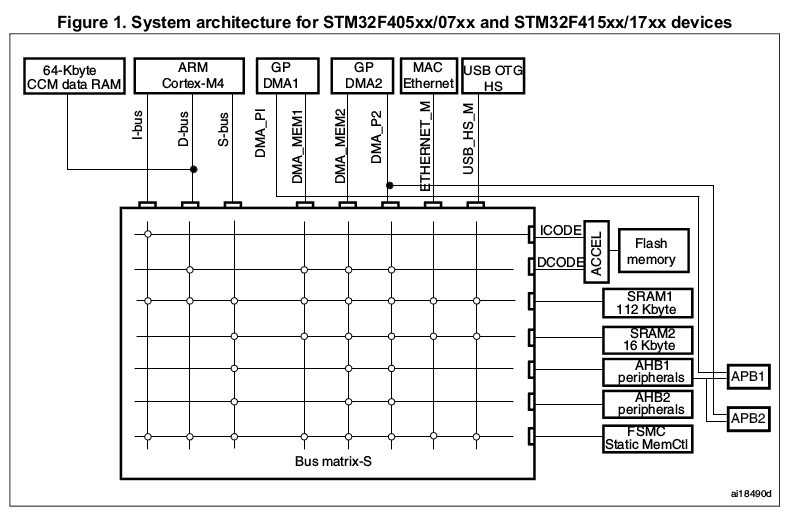
The large rectangle that dominates Figure 1 is the AHB matrix. It is the central interconnect of the STM32F407, determining which parts of the chip can talk to which others. For example, in part two, I used the matrix diagram to explain why we can’t use GPDMA1 to push pixels — it simply doesn’t have enough connections to the matrix.
Beyond that, the connections the matrix does have are not “fully interconnected.” Not all masters (along the top) can talk to all devices (at right). Data can only flow from a column to a row through a switch — shown in the diagram as a little white circle. If you can start at a master, trace down to a white circle, and then trace right to a device, then the master and device can communicate. Otherwise, no luck: there may be an overcrossing, but there’s no off-ramp.
AHB matrices like this are a common feature of Cortex-class microcontrollers, and when trying to get maximum performance from one, it always pays to study the matrix diagram closely, if one is available.
How to mess up the flow of pixels
To sustain a 40MHz pixel rate, we’re pumping a fair amount of data through the matrix — but we’re not using the whole thing. The flow of pixels only involves three players:
- GPDMA2.
- One of the AHB-attached SRAMs.
- A GPIO port, all of which are on the AHB1 bus.
The rest of the matrix is idle, or doing something we haven’t yet discussed.
I find it helps to visualize the flow of data across the matrix, like this:
I’ve scribbled a bit on Figure 1 here — the green line indicates the flow of data read from SRAM by GPDMA2, while the blue indicates writes to the GPIO port. We’re making use of two matrix switches, at the elbows of the two flows.
Ah, but what are all those little yellow icons? They’ve appeared atop some of the switches — specifically, all the rest of the switches in the two matrix rows we’re using.
These are matrix hazards.
You see, each device can be used by only one master at a time, and each master can only use one device at a time1. Put another way, only one switch in each row/column can be active at a time. If one master is using a device, and another master decides that they would like to use it, too, then we have a conflict2.
When I say “a master” here, I’m referring to a master port on the matrix, not a particular logical block inside the chip. Some blocks, namely CPU and DMA, own multiple master matrix ports.
And yes, it is entirely possible for a system with multiple master ports, like CPU and DMA, to conflict with itself.
It’s up to the matrix to decide who wins these conflicts, through a process called arbitration. A variety of strategies are possible: the masters could be prioritized; the requests could be handled in the order they’re received by the matrix; or the matrix could just pick a new master every cycle in a big circle.
Unfortunately, ST doesn’t specify the bus arbitration method used in the STM32F4, much less give us control over it3. However, from my experience, I know this much: if another master expresses interest in either SRAM2 or AHB1 while GPDMA2 is transferring, the matrix will begin interleaving the transfers of the two masters. Depending on the type of transfer being performed, each time the other master is given access to SRAM2 or AHB1, the GPDMA2 gets stalled by at least one cycle.
If they did, this article would be a lot shorter. CPUs with configurable bus arbitration, like the NXP LPC1788 (not 1768), are much easier to squeeze for every last drop of performance.
Conflicts cause stalls, and stalls cause late pixels. Slightly late pixels are effectively a phase shift, with respect to the 40MHz pixel clock; they will show as a slight fuzziness in the image on an LCD monitor or a nice CRT, and may not be visible at all on an older CRT. As pixels get later, the visual artifacts get worse, stretching sections of the display to the right. In extreme cases, this can shift video into the blanking interval, which can throw off the monitor’s automatic gain control and distort the whole frame.
So how late do the pixels get when we have a conflict? Well, it depends on the conflict. Let’s take a look at each of the conflicts that can affect m4vgalib’s scanout performance, and the methods I used to mitigate each one.
AHB1 port conflicts
While pixels are flowing, any other master that attempts to access AHB1 will interfere with the flow. Of the conflicts we’ll discuss, this one is the easiest to cause, for two reasons:
-
There’s a lot of useful stuff on AHB1. In particular, it’s the only path by which the CPU can access APB peripherals, via the AHB-APB bridges. AHB1, APB1, and APB2 together host most of the peripherals on this chip!
-
While the AHB bus itself is pretty fast, devices on the bus can slow it down by generating wait states. You can reach the SRAMs over AHB with zero wait states, but the GPIO appears to generate three, for four cycles total. Devices reached through the AHB-APB bridge are slower, because the APB buses in the STM32F407 can’t run as fast as AHB — so accesses to such peripherals cost 2x or 4x more, depending on the bus, plus their wait states.
Not only is it easy to trigger by accident, this conflict has the biggest negative impact on video quality. Unlike writes to memory, writes to GPIO are externally visible — so stalling them will stall the external signals4. The SRAM end of the transfer, on the other hand, can get nudged around by a cycle or ten with nobody being the wiser. (Though it can still be impaired by conflicts — more on that in the next section.)
This conflict is easier to trip in m4vgalib’s high-resolution modes because of my decision to run the DMA outside the control of a timer counter. However, it affects all high-rate DMA to an external interface, whether it be GPIO, SDIO, or something else, even when a synchronizing DRQ is used. If you want to get maximum throughput, you must be conscious of this matrix conflict!
At left, a polygon edge corrupted by a single AHB1 write during scanout. At right, the same edge without the conflict.
So far, I’ve only found one solution that works 100% of the time: only touch AHB1 during blanking intervals, either horizontal or vertical. This implies that any high-rate peripheral activity needs to be handled during hblank, and slower stuff can be done in vblank. m4vgalib does not enforce this in any way5. Instead, I’ve provided some tools to make it easy to do the right thing.
I’ve considered having m4vgalib use the Cortex-M4 Memory Protection Unit to block off AHB1’s address space, and then reveal it on entry to blanking periods. This would help application authors find access bugs faster, but it conflicts with the use of the MPU by most operating systems. Applications can surely do this for themselves!
m4vgalib lets applications synchronize to the start of the vertical blanking
interval with the vga::sync_to_vblank() function. Immediately after this
function returns, the application has a millisecond or so do work without
interference from the video driver. This is most often used to achieve
tear-free rendering, by e.g. flipping between buffers during vblank — but it’s
also a good opportunity to interact with low-speed peripherals. In the example
demos, it’s what I use to poll for user input: the buttons are attached to GPIO
lines, so to read them, I have to touch AHB1.
Synchronizing with the horizontal blanking interval is a harder problem. At
800x600, hblanks happen 37.8 thousand times per second, and whatever it is
that the application wants to do during hblank had better be complete within a
few microseconds. I assumed that applications would generally be written around
a main loop synchronized with vblank. So m4vgalib does not provide a
sync_to_hblank call. Instead, m4vgalib simulates an hblank interrupt:
applications can define a function named vga_hblank_interrupt, and m4vgalib
will call it early in the hblank, in interrupt context6. The
serial example
demo uses
this to handle serial input; Glitch uses it to output audio samples.
Specifically, vga_hblank_interrupt gets called from the PendSV
interrupt handler.
SRAM2 port conflicts
Any access to SRAM2 while pixels are flowing will limit the DMA’s ability to slurp pixel data, which can starve writes to the GPIO and thus cause visible artifacts. Compared to AHB1, this conflict is significantly harder to trigger in practice, both because of the different nature of the hardware on this end of the flow, and because of mitigation measures built into m4vgalib.
SRAM is faster than GPIO, in general7. The STM32F407’s SRAM is all zero-wait-state SRAM, meaning that it can complete a transfer in a single CPU/AHB clock cycle. However, SRAM accesses can stall the bus matrix for more than this would suggest, if the accesses are part of a burst.
If it were not, we would be able to sustain a 160MHz pixel clock. Some of the Cortex-M0+ parts have zero-wait-state GPIO, a trend that I hope eventually expands to the higher-end Cortex processors.
Bursts are uninterruptible sequences of transfers over the AHB bus: the matrix arbiter will not interrupt a burst to give a different master access. Bursts occur in the following cases:
-
Explicit burst transfers. You can configure the DMA controller to access memory (or anything, really) in bursts of 4, 8, or 16 transfers, multiplying the latency of the accesses by 4, 8, or 16 (respectively).
-
Implicit burst transfers due to unaligned access. The Cortex-M4 allows programs to perform unaligned memory accesses8. The AHB bus that connects the CPU to memory, however, does not — so the M4 must simulate unaligned accesses by making multiple, aligned, accesses. To make this appear as an atomic operation to the software, these transactions are combined into a burst. An unaligned read costs 2x; an unaligned write, 4x (a read-modify-write operation on two words of memory).
8Unaligned accesses can be disabled on the Cortex-M4, which removes the potential for this surprise. I leave it enabled in practice because it’s useful for packing data structures — and I find RAM to be more of a limiting reagent than CPU.
-
Implicit burst transfers due to bitbanding. The Cortex-M4 has a special area of its address space, the bitbanding region, that provides a sort of magnifying glass for SRAM: each word in the bitbanding region maps to a single bit in SRAM. This lets applications manipulate single bits in memory atomically without special instructions or intrinsics — m4vgalib leans heavily on this in its 1bpp line-drawing code. But bitbanding isn’t free. Like unaligned accesses, bitbanding is a fiction presented to software by the CPU; AHB knows nothing of it. Bitband writes, specifically, cause a burst of two transactions — one read, one write.
(You might suspect that a 64-bit access on Cortex-M4, e.g. through ldrd, would
also generate a burst transfer — but this does not appear to be the case.)
Even with these cycle-stealers lurking, it’s still pretty hard to bottleneck a transfer on the SRAM side — even with significant and repeated conflicts.
How hard is it? In preparation for writing this article, I ran an experiment.
I disabled all of m4vgalib’s SRAM conflict mitigation measures (described
below). I then ran the conway demo and used my Saleae Logic
Pro to monitor the video timing with 5ns resolution.
(conway produces the most AHB matrix traffic of all the example demos, so it’s
a good stress test.)
On average, I was able to elicit three cycles of conflict, or about 20ns, in each video line. This is less than a pixel; you might not even notice. But I noticed, because I am neurotic about this sort of thing. So I built in the following mitigation measures:
-
Use separate pixel RAM. You might have noticed that I’ve been talking about streaming pixels from SRAM2, and not the larger, more comfortable SRAM1. This is deliberate. m4vgalib accumulates pixels in SRAM2 during hblank and streams them from there, so that the application can make free use of SRAM1 (and CCM) without risk of a matrix conflict. (Reducing contention for SRAM1 also has another benefit, discussed in the next section.)
-
Discourage applications from placing stuff in SRAM2. The linker script used by the example demos distributes user data between CCM and SRAM1, leaving SRAM2 for the exclusive use of m4vgalib9. However, since it’s technically safe to use SRAM2 during blanking intervals, Glitch uses it to store audio mixing buffers. You can do this too — you just have to be careful.
9Because SRAM1 and SRAM2 are contiguous, it’s tempting to treat them as a single 128kiB RAM. Many vendor linker scripts do this by default. But because the two RAMs have different properties and are accessed through different matrix ports, this isn’t a good idea in high-performance situations.
-
Enable the DMA FIFO. Because SRAM is faster than GPIO, the DMA controller can “get ahead” on the SRAM side if it has somewhere to stash extra pixels. The FIFO provides such a place.
-
Use 32-bit accesses to SRAM. Yes, you could program the DMA controller to read a byte from SRAM, write a byte to GPIO, and repeat — but since the SRAM is natively 32 bits wide, that would waste ¾ of the SRAM bandwidth. Instead, m4vgalib has the DMA read SRAM into the FIFO in word-sized units, before dribbling them out to GPIO in bytes. (The DMA controller, like the rest of the system, does this in little-endian order.)
m4vgalib’s mitigation measures here are arguably redundant, a sort of belt-and-suspenders situation — either measures 1 and 2, or measures 3 and 4, do a pretty good job eliminating conflicts — but I didn’t want to have to worry about this ever again.
With all four measures active, I haven’t been able to create an SRAM-based conflict that interferes with the video in a way I can see or measure. And I’ve done some truly demented things to try to elicit one.
How to mess up an entire scanline
There’s another lurking beast that can damage video quality. There are a class of conflict that arise, not from masters fighting over the AHB matrix, but from the CPU tripping over itself. They can insert jitter into innocent-looking code in ways that can change from one compilation to the next! These are the last class of conflicts that I hunted down during the construction of m4vgalib, and the most subtle.
Fortunately, you can avoid them — once you understand them.
Flash wait states
The STM32F407 has quite a bit of Flash, by microcontroller standards — 512 kiB in my version. The chip boots out of Flash, and while it is possible to copy some code into RAM (specifically, SRAM1) and run it there, RAM is so much smaller that running code out of Flash is usually the right thing to do.
But Flash is slower than RAM. On the STM32F4 series, as you crank up the CPU speed, the Flash speed stays the same, limited by physics. At m4vgalib’s recommended CPU speed of 160MHz, Flash is six times slower than the CPU. This means it has to add wait states when the CPU accesses it — five, to be exact.
If every read from Flash took six CPU cycles, no performance-oriented programmer would want to run code from Flash — it would turn our beautiful 160MHz processor into a 26MHz processor! ST foresaw this, and provided a system they call the flash accelerator (Reference Manual section 3, “Embedded Flash Memory Interface”).
The flash accelerator maintains two small caches, similar to the L1 cache in a modern microprocessor: one for data, and one for code. More precisely, there is one cache for accesses made through the CPU’s I port, and one for accesses through the D port10; that’s basically the same as saying “one for code and one for data,” with one exception that we’ll discuss in a bit.
The CPU’s other port, the S port, cannot reach Flash. You can see this in Figure 1.
If the data you’re loading from Flash is in cache, the access is as fast as SRAM — one cycle, no wait states. If the data is not in cache, you pay the additional five cycle penalty.
In general, this is a really good thing. The flash accelerator contains prefetch logic that tries to have the next chunk of code waiting in cache before it executes11. Since the processor also tries to prefetch code before it’s needed, the two systems work together, and they work well: in general, moving code to RAM doesn’t make it run faster on an STM32F407.
If you’re using the A revision of the STM32F407, the prefetch circuit is broken. m4vgalib was originally developed on the A-rev, and as a result it puts more code in RAM than is strictly necessary. I’m gradually cleaning this up as time allows; any board you buy today should contain the newer Z-rev or 1-rev (ST counts strangely). Remember: always check the errata..
However, like any cache, it’s possible to sneak up on it and request some data it wasn’t expecting. The particular case of this that concerns us here: interrupt handlers.
I mentioned that there was an exception to the general rule that the I-port is used to fetch code: the I-port is also used to fetch vector table entries. This means that when an interrupt occurs, the CPU performs the following operations:
- Loads the vector table entry (I-port).
- Uses that address to load the first instructions of the ISR (also I-port).
- Writes the contents of 8 registers out to the interrupt stack (D-port).
(The D-port and I-port accesses can happen at the same time, a trick which is partially responsible for the Cortex series’ low interrupt latency.)
Now, if the vector table is in Flash, the vector table fetch hits the I-cache in the flash accelerator, and almost certainly misses. The cache only holds 1024 bytes, so if the program has executed at least 512 instructions since the last time this interrupt12 occurred, the vector table entry won’t be in cache. Bam, five cycles spent.
Or another interrupt whose vector table entry and/or ISR instructions share cache lines with the new interrupt.
If the vector table entry isn’t in cache, chances are pretty good that the ISR it points to has also fallen out of cache. Bam, five more cycles13.
In practice, these cycles of latency can overlap with the stacking of registers through the D-port, so they may be hidden.
The worst thing about this latency hit is that it’s unpredictable, in two ways. First, if an interrupt occurs frequently, it may hit cache — but if it slows down it will start taking longer. Second, if a rebuild of the software changes which 128-bit cache lines hold the data in question, it may either be cached more often — because nearby data is cached — or less often. So this 5-to-10 cycle penalty can actually change when software is recompiled.
m4vgalib contains a single latency-sensitive interrupt: the one generated at the end of hblank and used to start the flow of pixel data through the DMA controller. We can’t tolerate a variable latency of up to 10 cycles here, because it would shift the video to the right by just over two pixels! To avoid this, m4vgalib keeps both the vector table and the latency-sensitive interrupt handler in SRAM1.
m4vgalib goes one step further, actually: all of the code called on driver interrupt paths is in SRAM1. This isn’t to improve m4vgalib’s performance — as I said above, code in RAM rarely runs faster. No, m4vgalib does this to improve the application’s performance: to avoid polluting the I-cache on every interrupt.
If the interrupt stack also lived in SRAM1, the CPU would have to wait to stack registers until the vector table fetch and code fetch were complete. But remember that registers are stacked through the D-port, which has access to the 64 kiB Closely Coupled Memory, or CCM (upper left in Figure 1). m4vgalib places the interrupt stack in CCM to avoid this conflict.
Let’s do the time warp again
Even with your vector table and ISR in SRAM, you may still observe variation in interrupt latency.
One of the factors is one I’ve beaten to death in this article: AHB matrix conflicts. Accesses from the CPU to Flash and SRAM have to traverse the matrix, so the same factors that can affect DMA can also affect interrupt latency. Fortunately, the devices accessed during interrupt dispatch are separate from the ones m4vgalib uses for scanout, so interrupt activity doesn’t directly interfere with DMA.
To visualize this, here’s another matrix diagram. The green and red lines still indicate the flow of pixel data. The new aqua line shows the flow of registers from the CPU to the interrupt stack (in CCM, because that’s where m4vgalib puts it), and the purple line, the flows of vector table and instruction data into the CPU (assuming it comes from SRAM1, as in m4vgalib).
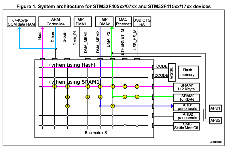
These flows do not conflict. However, two classes of conflict can still arise:
-
Implicit bursts. Recall from earlier in this article that unaligned accesses and bitbanding both generate AHB burst transactions. If an interrupt occurs while a burst transaction is underway, any part of the interrupt dispatch process that conflicts with the burst is delayed. In practice, this typically means an unaligned access in SRAM1 delaying the fetch of the vector table entry from SRAM1.
-
Flash accesses in the application. If code issues a Flash access that misses cache, it takes a five-cycle penalty — and so does anything else trying to use the same resources. This not only means that accesses to the Flash would be delayed, but that any accesses using the same port on the CPU would be delayed. So an application running from Flash can delay m4vgalib’s interrupt handlers, even though they live in SRAM, because the vector table fetch must wait for the wait states on the I-port to elapse.
Finally, there’s a subtle property of the Cortex-M4 processor that can actually cause interrupt latency to unpredictably decrease: tail chaining. If a previous interrupt (perhaps handled by the application) is ending just as a new interrupt is arriving, the processor effectively jumps from one ISR to the other, and doesn’t bother stacking registers again. This shaves six cycles off the interrupt latency — but only when two interrupts occur close together!
This all seems like a bit of a pickle. I don’t want to impose restrictions on how applications are built: they should be allowed to run from Flash, and they shouldn’t have to idle waiting for m4vgalib to take a latency-sensitive interrupt. Moreover, the tail-chaining timewarp is almost impossible to predict. What to do?
m4vgalib eliminates both sources of latency through a mechanism I call the
“shock absorber.” The idea is simple: just before a latency-sensitive interrupt
arrives, schedule a second interrupt, at a slightly lower priority. This
interrupt’s handler just executes the ARM wait-for-interrupt instruction, or
wfi — idling the CPU. This gives any (CPU-initiated) AHB transactions time
to complete before the latency-sensitive interrupt arrives. When it arrives, it
will preempt the wfi instruction, which will resume (returning from the shock
absorber) when the other ISR completes. Because of the wfi, we know that the
CPU’s I-port and D-port are both idle in time for the vector fetch.
In the specific case of m4vgalib, just before the timer interrupt fires to start DMA, a second timer interrupt fires and runs the shock absorber code to idle the system.
This is probably the strangest thing I’ve done in m4vgalib14, but it works great — it eliminated the last detectable source of jitter in the system.
I have done stranger things elsewhere.
Coming Up Next
That concludes our whirlwind tour of the forces that can corrupt video output on an STM32F407, and the mechanisms m4vgalib uses to mitigate them. In the next part, we’ll move up a level and look at m4vgalib’s rasterization framework. If this post was too heavy on hardware for you, the next post may be more your speed: parts will be written in assembly language! Stay tuned.