1. Fast setup
If you’ve done this before and just need a refresher, if you’re very comfortable with embedded electronics, or if you don’t like pictures of dinosaurs, here’s the short version of the instructions:
-
Install a header on J7: the serial connector.
-
Connect J1: the keypad connector to your keypad, probably by installing another header or direct wire-to-board. (If you’re going to connect Keypad Go in a way that will make it hard to access the back of the board, configure the jumpers first.)
-
Connect a 3.3V serial interface to J7.
-
Provide 3-16V on J7 pin 1 (5V from the power pin of a 3.3V serial cable will do nicely).
-
Connect to the serial interface at 19200 8n1 (19200 baud, 8 bit, no parity, 1 stop bit).
-
Tap the RESET button and follow the instructions that appear.
Then, hop to the section describing the serial protocol to interface the configured keypad to your project.
The next section will say the same thing with more words and pictures.
2. Getting started
To complete the setup process, you will need to be able to interact with Keypad Go through its serial port. This means you’ll need a way of receiving its output and typing responses back. There are many ways you could do this, and this guide assumes that you’ve either already got one you like, or are willing to figure one out by messing around on the internet. Some examples might include:
-
Plugging a 3.3V USB-serial cable into your computer and running a program like
screen,putty, orminicom. (If you are on Windows, make sure you have a driver for your cable.) -
Using jumper wires to connect Keypad Go to the native UART pins on a Raspberry Pi, and running something like
screenorminicomon the Pi overssh. -
Using a 3.3V Arduino as a Very Fancy Serial Port by way of the
SerialPassthroughexample (built in to the Arduino IDE).
In addition to the parts for the serial connection, you will also need to have available:
-
A 4-pin strip header (or wires, if you prefer) for the serial connection.
-
Something to connect Keypad Go to your keypad — generally an 8-pin strip header, but there are many keypads out there.
-
Basic soldering tools.
(If you requested them at checkout, the header strips were included in the bag with Keypad Go. Otherwise, any 2.54mm pitch header or connector will do.)
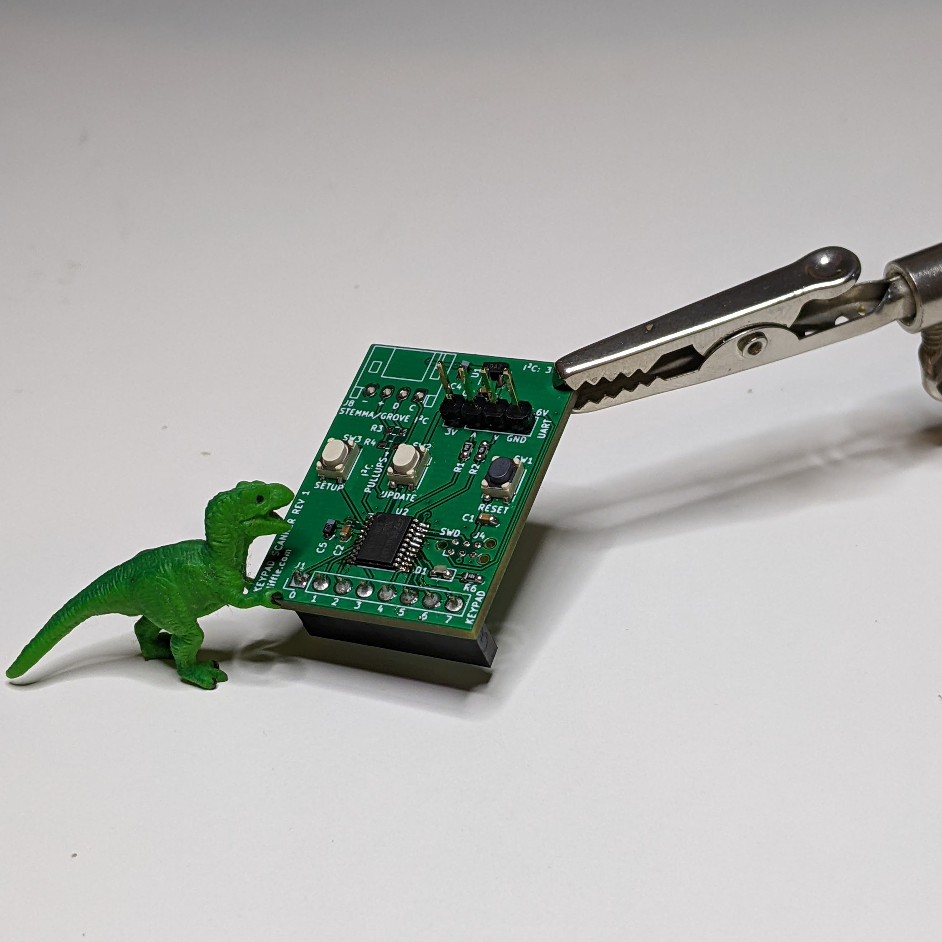
The Keypad Go PCB is pretty small, and I’m kind of big and clumsy, so for the demonstration photos below I’ve enlisted the help of my trusty lab assistant, Gargantua McStompers.
2.1. Step One: Install headers
There are two headers you’ll want to solder on.
J7 (serial) should be a four-pin header appropriate for your serial interface, generally a pin header. J1 can be any header appropriate for your keypad.
In the photo below, Gargantua has chosen a simple pin header for the serial connector, and an 8-pin socket for the keypad connection. This is the most flexible option since it will let her move Keypad Go to a different keypad later, if she needs to.
(Please disregard the missing I2C connector, she’s using a prototype board.)
You can also solder wires directly to J7 if that’s your style.
2.2. Step Two: Attaching the board to your keypad
Keypad Go is mostly designed around cheap commodity keypads that look something like this:
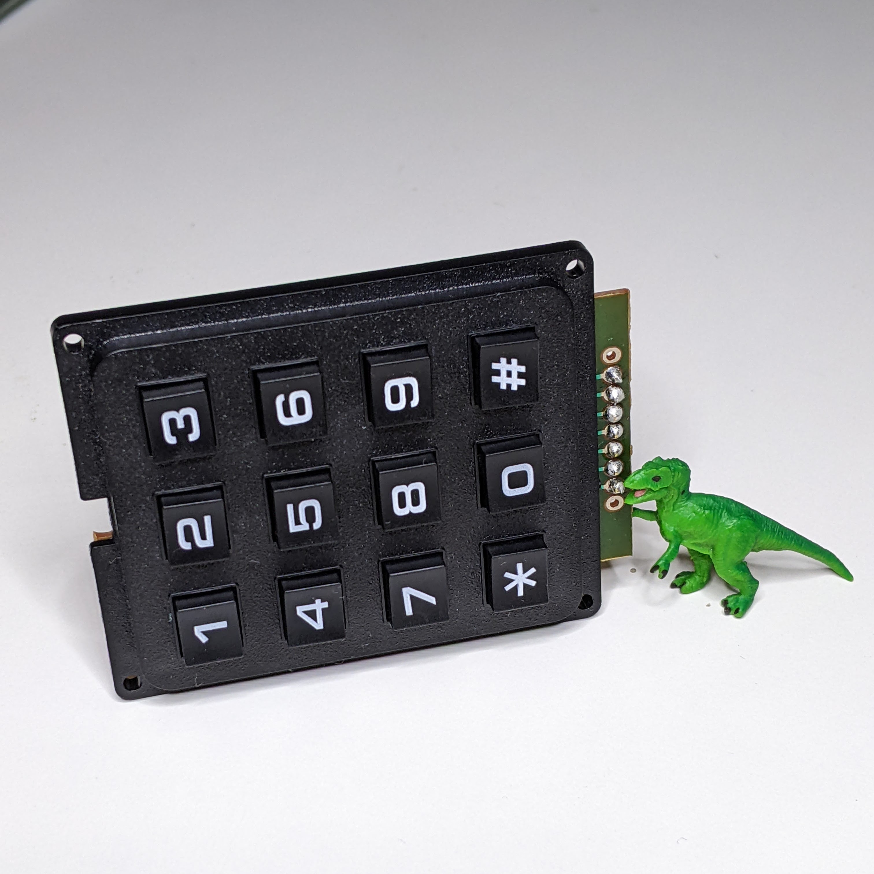
Keypad Go is designed to solder to the row of pads at the bottom. Here, Gargantua has already installed a header pointing to the back. Most keypads only have metal on one side of their circuit board (the front), so soldering a header pointing the other way is hard. Plus it would block the keys. Don’t do that.
Note that the holes on either end are not connected. If you look closely you’ll see why: unlike the seven holes in the middle, the holes at either end don’t have a metal trace connecting them to the rest of the board. Those holes are not electrically connected. You can wire them up if you like, they just won’t add anything. Gargantua has elected to leave them free.
The other side of Gargantua’s keypad now looks like this:
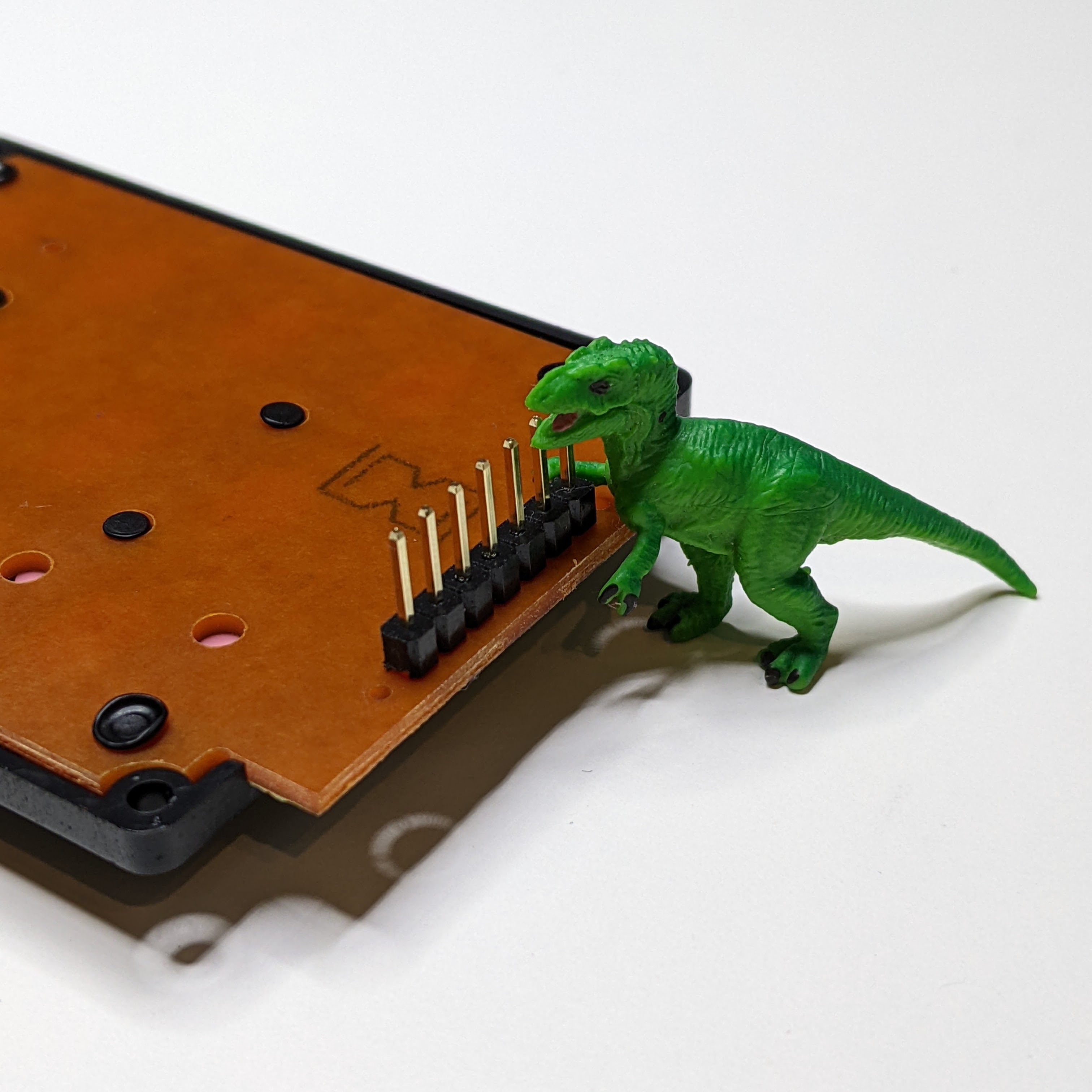
Now we need to plug the two pieces together. If you’re planning on connecting the keypad in a way that will make it hard to remove — like soldering it directly to the board — make sure you read the text on the back of the board and the section on jumpers in this manual first. You may want to change the default jumper settings, depending on what you’re planning on doing.
Plug the two pieces together. (Or solder them together, if you’re really committing.)
| Gargantua has reminded me to mention that, if your keypad has fewer pins than Keypad Go, it doesn’t matter which ones you wire up. Keypad Go will figure out if some of its connections are unused, and ignore them. |
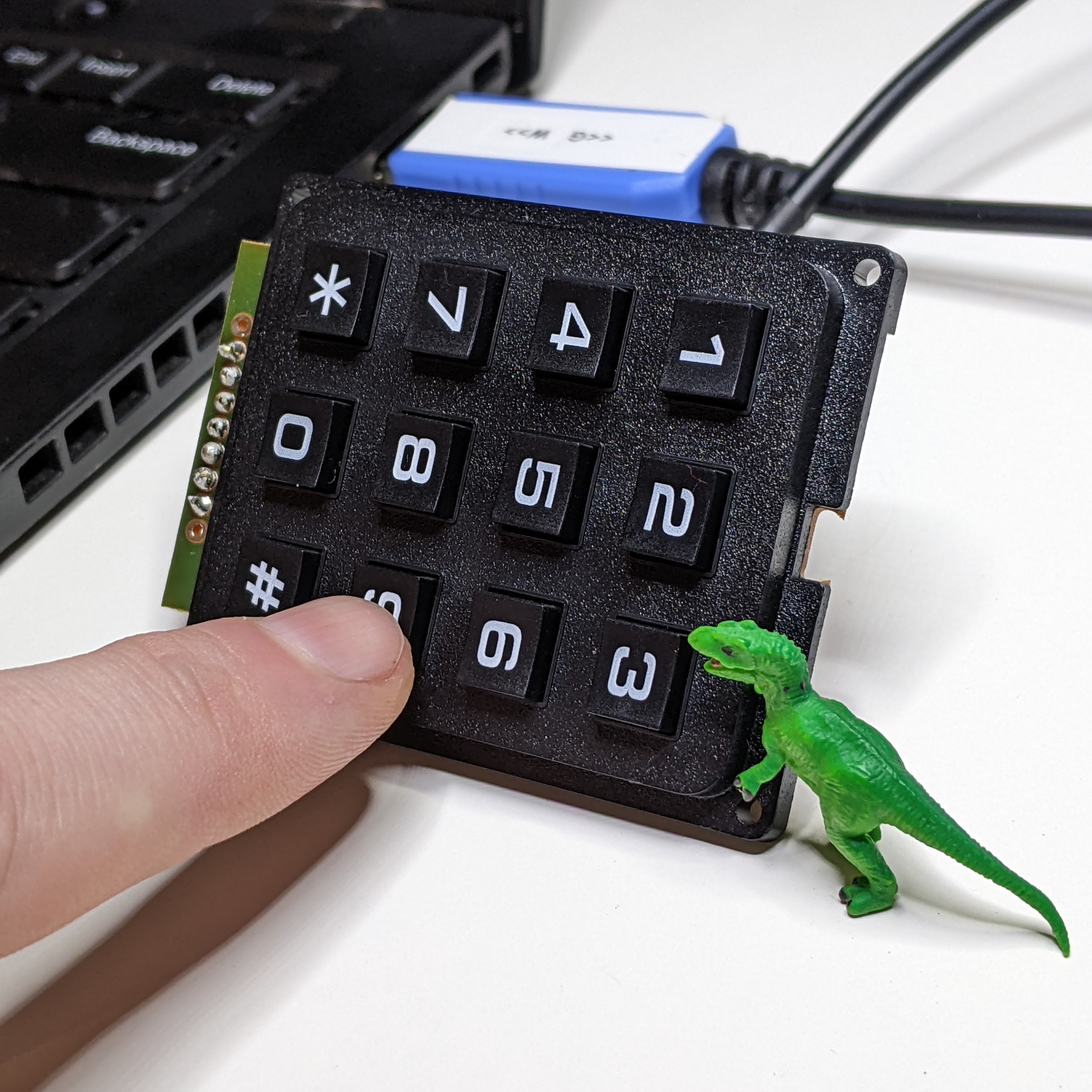
2.3. Step Three: Connect a TTL serial interface
The most common tool to use for this step is a 3.3V USB-serial cable. Gargantua is using a popular cable with loose color-coded connectors on the end, so that she can connect them in whatever order is required. (Gargantua checked the cable’s datasheet to confirm the wiring order. The colors of your cable may be different! Be like Gargantua: read the datasheet.)
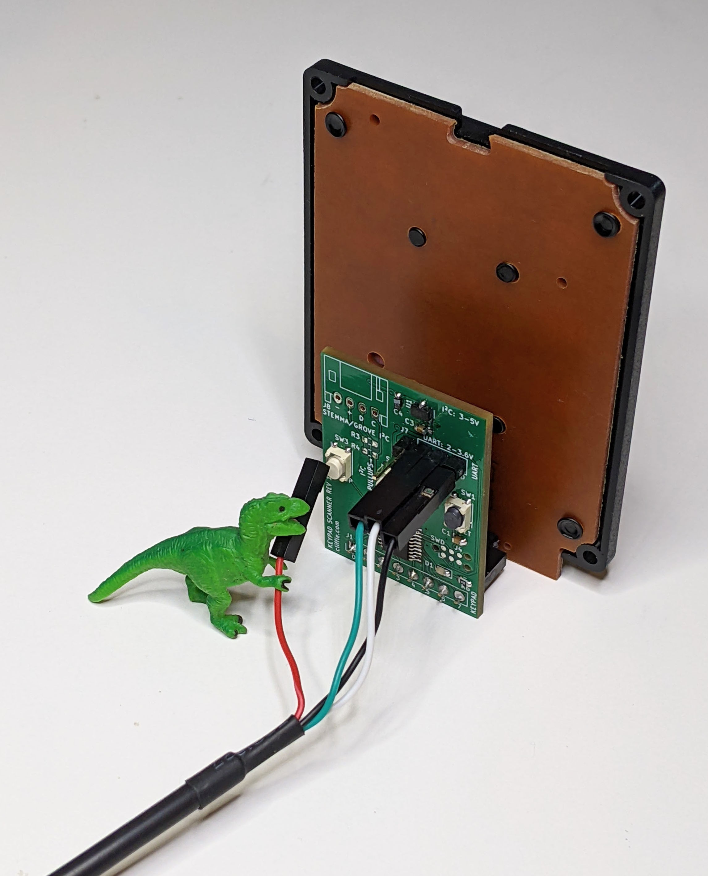
You will need to connect at least GND and data/in out to the serial connector J7. Gargantua is also hooking up the power connection from her cable, which is the easiest way to get started with Keypad Go. Most USB-to-serial cables provide 5V on one wire, which will do nicely for powering Keypad Go. (Ignore the part where the power pin is labeled 3V, that’s a mistake on my part.)
Here’s a drawing to help you match your cable to the connector if the colors differ:
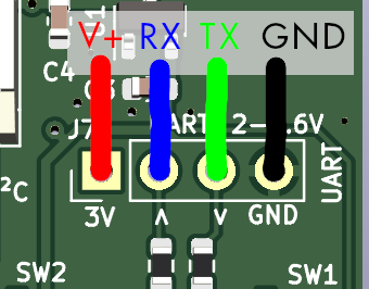
Pin 2, which is labeled with a small arrow pointing toward the connector, is where data comes out of the Keypad Go. This should be connected to the RX pin on your cable.
Pin 3, which is labeled with a small arrow pointing away from the connector, is where data goes into the Keypad Go. This should be connected to the TX pin on your cable.
| TTL USB-serial cables come in 3.3V and 5V varieties. Keypad Go is designed to work with 3.3V cable, but may work with your 5V cable, depending on the type. USB cables tend to provide 5V on their power output pins even if they’re 3.3V cables. This is fine for Keypad Go. |
| Do not connect an RS232 cable to Keypad Go. RS232 uses higher voltages that may damage the circuit. |
2.4. Step Four: Open a serial terminal
In setup mode, Keypad Go communicates over asynchronous serial at 19,200 baud, 8 data bits, 1 stop bit, and no parity (19200 8n1). Connect the other end of the TTL serial cable to your computer, or phone, or Pi, or antique terminal, or whatever, and configure it to speak that way.
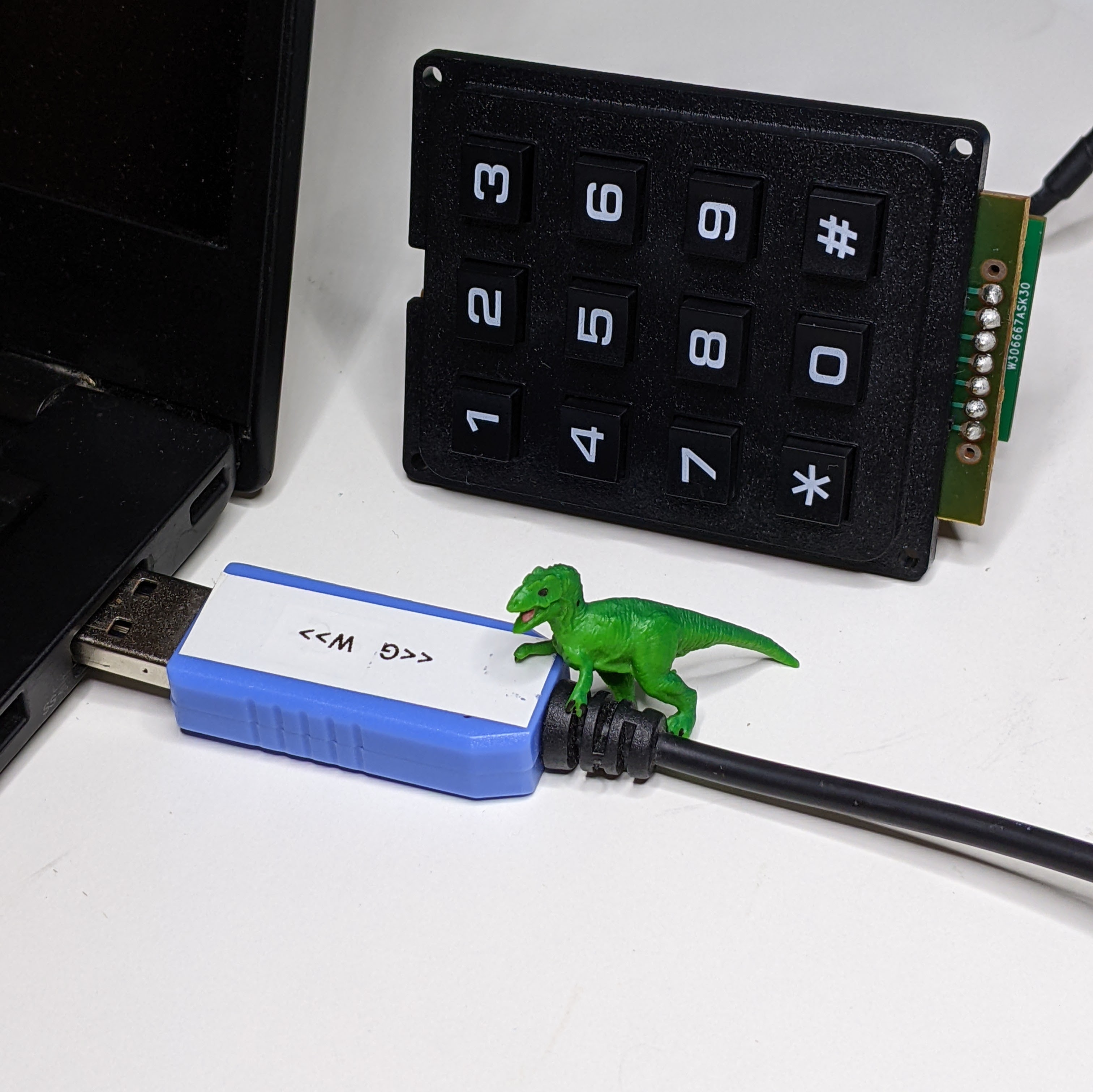
To see if things are working, tap Keypad Go’s RESET button. You should see output in your terminal.
| Make sure flow control is disabled — both software and hardware. |
| If you have previously configured Keypad Go, you won’t see any output when you tap RESET. You can put Keypad Go back into setup mode by holding the SETUP button (SW3) when you tap RESET. |
If your terminal is configured correctly, you should see Keypad Go printing
instructions, starting with SETUP MODE. Follow the instructions. Keypad Go
will ask you to press buttons on the keypad at certain times:
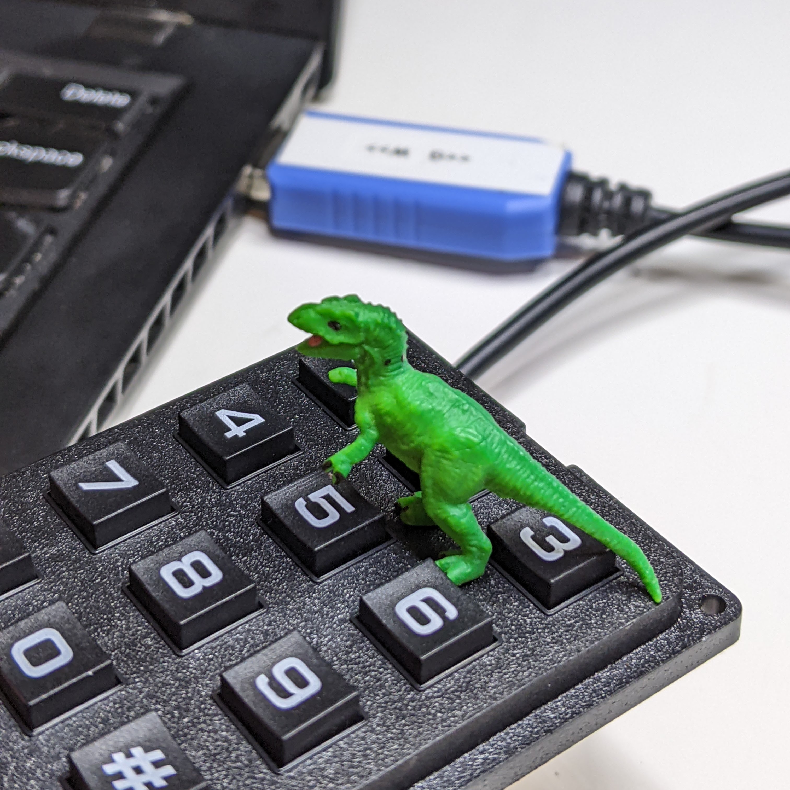
If, like Gargantua, you are much smaller than the keypad, ask a giant friend for help.
The next section discusses the setup process in more detail.
3. Setup mode
| If you have previously configured Keypad Go, you can access setup mode by holding the SETUP button (SW3) when you tap RESET. |
When setup mode starts, it will print (in your terminal):
SETUP MODE
Firmware version: 1.0.2

Press+hold any keypad button.
Type ESC here if no more.
(Your firmware version may differ.)
In order for Keypad Go to determine the wiring of your keypad, you’ll need to press one button at a time. The order doesn’t matter. Each time you press a button, Keypad Go will respond with something like:
Found:
1 -> 2*
2 -> 1

Please release button.
The numbers indicate which pins connect when the button is pressed. In this case, pressing the button was found to short pins 1 and 2 on the keypad.
| If you have a larger keypad that uses diodes, you will only see one set of numbers at this point. |
Once you release the button, Keypad Go will prompt:
Type the key's character here:
Type the character you want to map to that button into your terminal. For
instance, if you’ve pressed the keypad button marked "1", you would press the
1 key. This will cause Keypad Go to reply
OK
…and then repeat the request for you to press a button. Once you’ve mapped all
the buttons, hit ESC in your terminal to tell Keypad Go that you’re done.
Keypad Go will then print details about the keypad schematic it’s detected, followed by
Save? (Y/N)
If you enter Y the configuration will be saved in flash. If you enter N, the
configuration will be discarded and you’ll have to re-enter setup mode if you
want to try again.
Either way, Keypad Go will then start a "demo mode" that lets you try out the keypad. In demo mode, Keypad Go will print descriptive messages of any key activity it senses. Poke some keys — if anything seems wrong, restart setup.
Once a configuration is saved, Keypad Go will use it until you replace it, even when power is lost.
4. How to use Keypad Go after setup
Once set up, connect either Keypad Go’s serial interface or I2C interface.
| To use both interfaces at the same time, you have to make a change to the board. See JP1/JP2: power options. |
If you’d ever like to change the configuration, or attach the board to a different keypad, you can always re-enter setup mode. This won’t affect your configuration unless you save the results.
4.1. The serial protocol
If you connect the serial interface, Keypad Go will send the character you configured for each key during the setup process when the key is pressed. When the key is released, it will send the same byte with the high-order bit set. If you only care about keys going down, you can ignore bytes with the high-order bit set.
4.2. The I2C interface
If you connect the I2C interface, Keypad Go will buffer keypresses and let you read them out at your leisure. The main requirement is that you need to keep up with any keypresses, because there’s a limited amount of buffer space and it can fill up.
| The I2C interface includes pullup resistors, and pulls the data lines up the voltage on the I2C connector power pin — which is generally being produced by whatever I2C host you’ve connected Keypad Go to, but is also connected to the serial connector by default. This has two implications. First, if you’re powering the board from 5V, this means your I2C pins will use 5V levels. Second, if you’re attempting to use both the serial and I2C interfaces simultaneously, power will be connected across both connectors. Make sure that’s okay with whatever you’re connecting to, and consider changing the jumper setting if it isn’t. |
Keypad Go responds at the 7-bit I2C address 0110011, which, depending on
the convention used by your I2C library, might be written as 0x33 or
0x66. Check whether your library wants a 7-bit (i.e. reasonable) address or an
8-bit address with its least significant bit ignored (i.e. unreasonable).
| The I2C address is not currently programmable, but adding this would be straightforward if someone needs it. Please send me a note! |
The I2C protocol is almost as simple as the serial protocol. If you read data from Keypad Go, you will receive buffered keypresses — the same bytes that would be sent out the serial connection. Keypad Go reserves some space for key events (up/down pairs). If your user hammers keys faster than you read them, the buffer will fill up, and key events will be lost.
| Versions of the firmware before 1.0.3 (units shipped before May 2024) have space for 7 up/down pairs. 1.0.3 and later have space for 32 up/down pairs. If you’re running an older version and need more buffer space, you’ll need to update the firmware. |
You can detect this by whether the buffer contains any zeroes at the end. After all buffered keypresses are sent, Keypad Go will send zeroes until you stop asking. So, if there is a zero in the first 32 bytes of the response, you have received all the key events and nothing was lost. Hooray!
If you read 32 bytes and find no zeroes, it means the buffer filled up and key events may have been lost. Your project may want to do something about this — for instance, if you track key up/down state (rather than only responding to key-down), this would be a good time to clear that and treat all keys as "up."
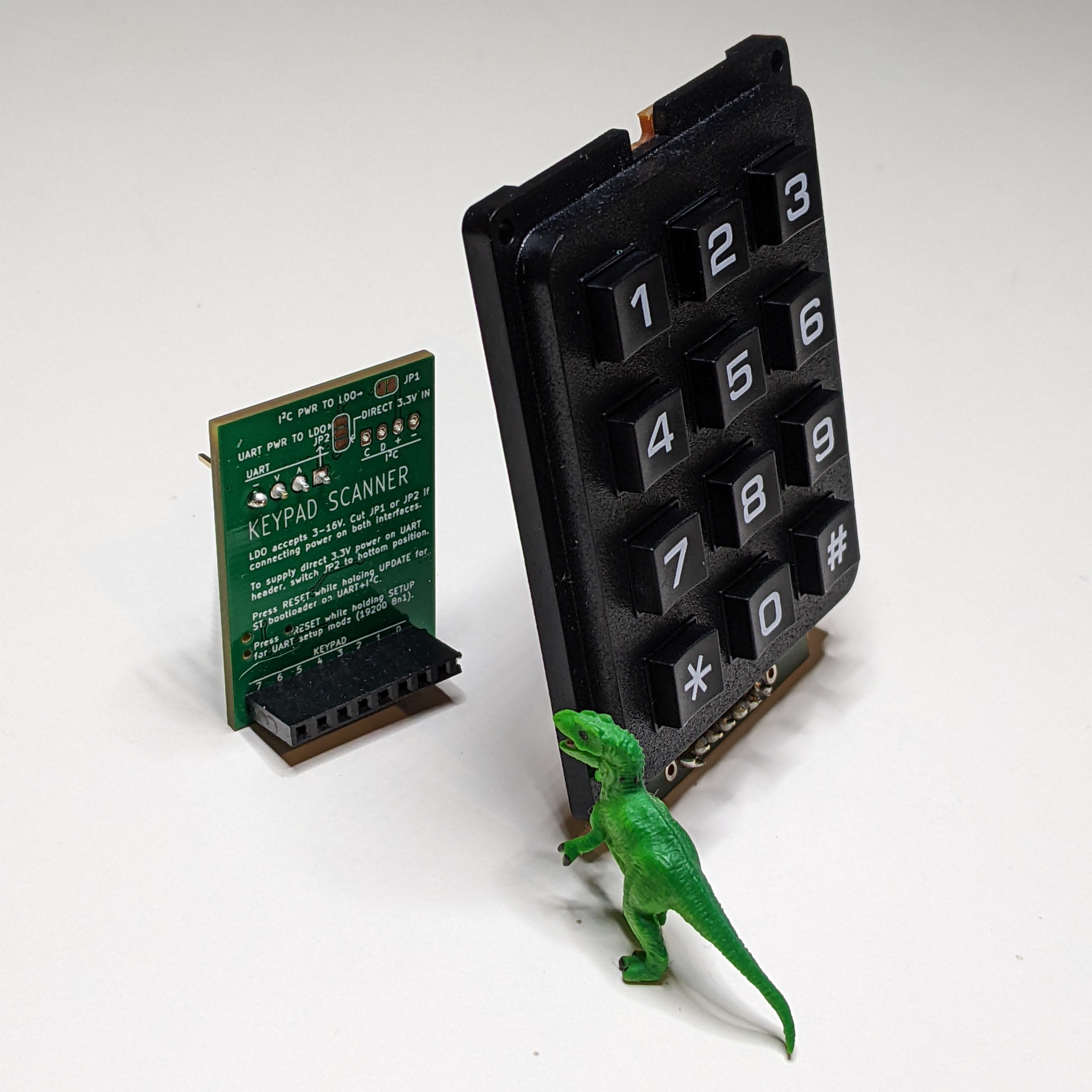
5. A tour of the board
The Keypad Go has two sides. The top side is the one with all the components stuck to it. The bottom side is flat and has some instructions written on it.
This section will walk through the main user-facing bits of the board to help you locate things.
5.1. Connectors
5.1.1. J1: the keypad connector
J1 is an 8-pin 2.54mm-pitch header designed to connect to a keypad. Common keypads have a seven-to-ten pin row of contacts with this same spacing, generally at the bottom; use the included strip of header pins (breaking it to make it shorter if required) to connect J1 to the contacts on your keypad. (Note that the pads on the very end of many keypads are vestigial no-connects!)
The pinout of this connector doesn’t really matter, because the board can remap these lines freely once it discovers your keypad’s wiring. See the setup mode section for more information.
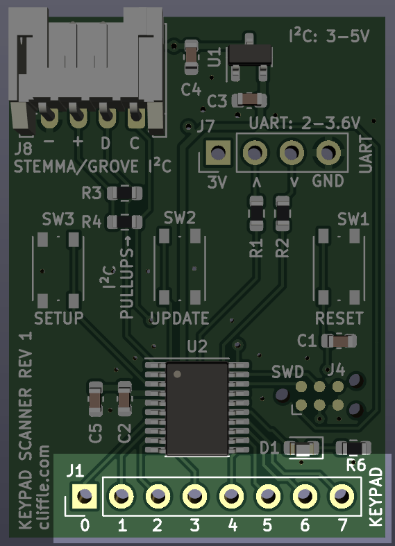
5.1.2. J7: the serial connector
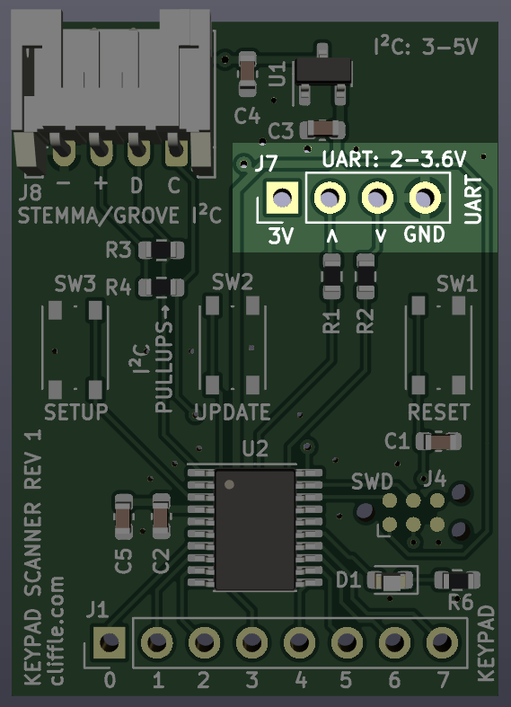
J7 is a 4-pin 2.54mm-pitch header that carries asynchronous serial data at 3.3V levels. This plays two roles:
-
It’s how you set up the Keypad Go for a particular keypad, and
-
It’s the easiest way to get keypad activity out of the Keypad Go and into your application.
In setup mode this connector acts as an interactive terminal interface. Once setup is complete, it runs the serial protocol.
Pinout:
| Pin | Name | Notes |
|---|---|---|
1 |
VBUS |
Power input, 3-16V depending on JP2 |
2 |
OUT |
Serial data out at 3.3V, connect to RX on your application or UART cable. |
3 |
IN |
Serial data in, connect to TX on your application or UART cable. |
4 |
GND |
Connect to ground in your application or cable to ensure a common reference voltage. |
| Keypad Go’s serial levels will work with some 5V serial interfaces — the IN pin will tolerate 5V, but the OUT pin is always 3.3V. Check the "minimum input High voltage" (or Vih) for your cable or microcontroller to see if 3.3V counts as high. |
5.1.3. J8: the I2C connector
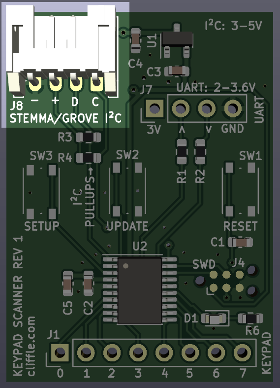
J8 is a 4-pin JST PH connector that carries I2C data and power. It is intended to be compatible with the Adafruit STEMMA and Seeed Studio Grove systems. This provides an alternate way of getting keypad activity out of the Keypad Go if your application is already using I2C.
The I2C interface on Keypad Go is 5V tolerant, so you can use this connector whether you’re on a 5V or a 3.3V I2C bus.
By default, power connected to this connector will be fed to the voltage regulator and adapted for use by Keypad Go’s CPU; if you don’t want this to happen, see (TODO).
Note that the power pin of this connector is directly connected to the power pin on J7 (the serial connector). This means that, out of the box, you must not connect both these connectors at the same time. You can fix this by choosing to take power only from one side or the other, using the jumpers on the back of the board.
Pinout:
| Pin | Name | Notes |
|---|---|---|
1 |
SCL |
I2C clock signal. |
2 |
SDA |
I2C data signal. |
3 |
VBUS |
Power fed to the voltage regulator (by default). Also connected to J7 (by default). |
4 |
GND |
I2C bus and power supply ground. |
5.2. The buttons (SW1, SW2, SW3)
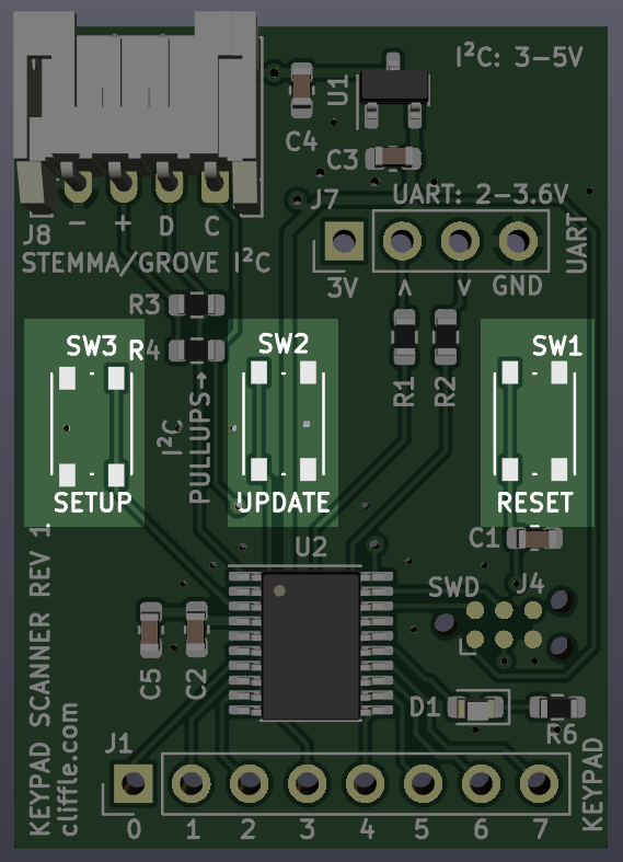
SW1 is the reset button. Pressing it resets Keypad Go and causes it to reload the configuration (if any) from flash. You can use this to abort setup mode if you want.
You can change Keypad Go’s behavior by holding one of the other two switches while pressing reset.
-
If you hold SW2 (UPDATE) and tap reset, Keypad Go will reboot into the bootloader to allow firmware updates through the UART or I2C. To get out of the bootloader, tap reset again.
-
If you hold SW3 (SETUP) and tap reset, Keypad Go will enter setup mode.
5.3. The configurable bits
5.3.1. R3/R4: the I2C pullup resistors
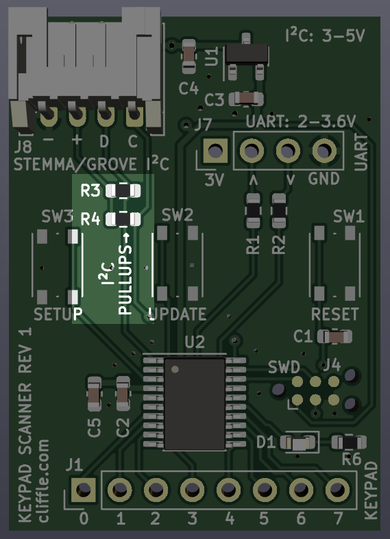
Keypad Go comes with pullup resistors installed on the I2C signals, which is normal for a device in the Stemma or Grove ecosystems. If you have pullup resistors somewhere else, you can remove R3/R4.
5.3.2. JP1/JP2: power options
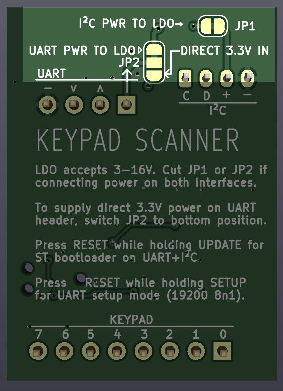
JP1 determines whether the power pin on the I2C connector can be used to power the board. When JP1 is bridged (default setting), the I2C connector is connected to the voltage regulator. Cutting JP1 disconnects it.
JP2 determines the role of the power pin on the serial connector.
-
If JP2 is bridged between the two top pads (default setting), the power pin on the serial connector is connected to the voltage regulator. This makes it safe to feed 5V into that pin, but causes it to conflict with the I2C connector.
-
If JP2 is instead bridged between the bottom two pads, the power pin on the serial connector is connected directly to Keypad Go’s internal 3.3V rail. In this mode, it’s only safe to supply between 2 and 3.6 volts to the serial connector, but it no longer conflicts with I2C.
-
If JP2 is open on both sides, then the power pin on the serial connector is disconnected.
So, if you would like to use both the I2C and serial interfaces at the same time, you need to choose which one is responsible for powering the board, and disconnect power from the other.
| Jumper setting | Meaning |
|---|---|
JP1 bridged (default), JP2 1-2 (default) |
VBUS connected to both I2C and serial power pins, which are shorted together. VBUS provides regulator input. This requires VBUS in the range 3.6 - 5V (though 3.3V seems to work). If you use both interfaces in this configuration the power lines will be shorted, make sure that’s okay (ideally only one of the two interfaces is providing power). |
JP1 bridged (default), JP2 2-3 |
VBUS connected to I2C power pin and provides regulator input (3.6 - 5V). Serial power pin is directly connected to 3.3V regulator output. You can power the whole board from 3.3V on the serial connector in this configuration. Be careful providing 3.3V on serial and power on I2C simultaneously in this configuration, because current will flow into one power supply or the other if the voltages differ (and they will). |
JP1 bridged (default), JP2 open |
VBUS connected to I2C power pin and provides regulator input (3.6 - 5V). Serial power pin is disconnected. Board must be powered over I2C. Safe to use both interfaces. |
JP1 open, JP2 1-2 (default) |
VBUS connected to serial power pin and provides regulator input (3.6 - 5V). I2C power pin only provides voltage for I2C pullups, thus setting the I2C signal voltage level. In this configuration it’s safe to use both interfaces, powering Keypad Go from the serial connector. Do not use this configuration with only I2C connected, as it will back-power Keypad Go through its I2C pins and things won’t work right. |
JP1 open, JP2 2-3 |
VBUS and regulator disconnected. Serial power pin connected directly to processor power input (2 - 3.6V). I2C power pin provides pullup voltage (2 - 5V). This is the lowest-power mode if you’re only using the serial interface. Do not use this configuration with only I2C connected, as it will backpower Keypad Go through its I2C pins and things won’t work right. |
JP1 open, JP2 open |
Processor power is not connected. Connecting either interface will back-power the processor through its I/O pins and things won’t work right (and may be damaged). Don’t use Keypad Go in this configuration. |
-
To source power only from serial, cut JP1 and leave JP2 intact.
-
To source power only from I2C, cut JP2’s top bridge.
| if you choose to bridge the bottom two pads of JP2, make sure to cut the bridge between the top two! If you short all three pads of JP2 you will destroy the voltage regulator. |
6. Known issues in v1
-
The label on J7's power pin says 3V, which is misleading since it’s not configured in direct 3V power mode by default. (The label above the connector describes the signaling voltages, and is correct.)
7. Firmware and updating
7.1. Figuring out what version you’re running.
To determine what firmware version you’re currently using, connect Keypad Go to your computer using a serial cable (like you did to initially run setup) and re-enter setup mode. The banner will print the current firmware version if you’re running 1.0 or later. (On 0.9, it won’t print a version.) It is safe to do this even if you have already configured Keypad Go, because setup mode won’t overwrite your configuration unless you tell it to.
| Applying a firmware update carries some risk. Make sure Keypad Go is connected to reliable power during the process. If you get any errors during the update, try it again without resetting. If Keypad Go reboots with partially written or corrupt firmware, it may not boot into bootloader mode next time. This is a limitation of the STM32G0/C0 series, which don’t expose a useful hardware pin for forcing bootloader access. If this occurs, see the next section. |
7.2. Using the Updater (recommended)
The easiest way to update the firmware is using the Keypad Go Firmware Updater. This is an open source, cross-platform program that automates the process of detecting which board variant you’re using, loading the correct firmware, and doing a basic system test to ensure that it’s working.
To use the Updater you will need to have a Rust toolchain installed.
Download the firmware package here:
Then, check out the Updater from the link above and run:
cargo run -p <SERIALPORT> keypad-go-firmware-1.0.2.zip
…replacing <SERIALPORT> with the name of your system’s serial port or
USB-to-serial adapter.
If you’d like to use firmware you’ve built yourself, the package.sh
script in the firmware repo will produce this style of firmware package for use
with the Updater.
|
7.3. Using the raw bootloader
If you can’t (or don’t want to) run the Updater, you can also feed firmware directly into the bootloader. This process requires significantly more care.
Depending on which batch you received, Keypad Go has one of two microcontrollers: either an STM32G030 or an STM32C011/31. The variant is indicated in three ways, from easiest to hardest:
-
The box included a card telling you which one you had, in large, easy-to-read letters.
-
The board itself will be marked. On older revisions there is a hand-scratched letter, next to the serial number, reading C or G. On newer revisions, there is a checkbox near the serial number.
-
On the CPU (U2), in tiny black letters on a black background, it will say C0 or G0. You’ll probably want a magnifying glass.
The firmware images for the two processors are sliiiiightly different, so, please make sure you use the right one!
Download the firmware package linked above for use with the Updater. This package is just a ZIP file. If you unzip the package, it contains files named for each CPU model.
-
C011xx.binis the firmware for STM32C0x1-based boards. (It’s also namedC031xx.bin; these files are the same.) -
G03xxx_G04xxx.binis the firmware for STM32G030-based boards.
Keypad Go accepts firmware updates on either of its interfaces using the standard ST ROM bootloader. However, if it senses voltage on the I2C pullups, it will listen exclusively to I2C. (This is an ST behavior, not specific to Keypad Go.) Disconnect any I2C cable if you want to update firmware using the TTL serial interface.
| On batch 1 boards, to use the TTL serial interface for a firmware upload, you will need to set the jumpers on the back to disconnect serial power from I2C. Either cutting JP1 to leave it open, or switching JP2 to directly provide 3.3V through serial, will work. |
To boot Keypad Go into ST’s bootloader:
-
Press and hold the UPDATE (center) button.
-
Tap the RESET button.
-
Release the UPDATE button.
The board will now respond to the first interface where it notices a connection. You can use any tool compatible with ST’s bootloader to perform the upload. This Python script seems to work and is pretty cross-platform.
7.4. Recovery using SWD
If Keypad Go’s firmware is damaged or corrupted, it won’t boot, either normally or into the bootloader. This can happen if you upload a file other than the correct firmware when performing an update.
Keypad Go has a SWD pogo-pin footprint (J4) that matches the layout used by Tag-Connect TC2030-CTX cable. You can connect to it using a compatible pogo-pin cable, or (in an emergency) by soldering fine wires directly to the pogo pins. At that point, you can use a SWD programming interface (such as an STLink) and software (such as OpenOCD) to reboot and reflash the microcontroller.
If you have a recent OpenOCD (say, 0.12.0) and arm-none-eabi-gdb installed,
and you are using an STLink, the firmware repo contains compatible configuration
files. You can run openocd from the repo, and then run cargo run --features
XXX from a different terminal. Note that the XXX depends on which processor
you’ve got; see the firmware repo for details.
I can’t give exact directions or help with this, because your setup is likely very different from mine. Try not to corrupt the firmware. Contact me if you need help.
8. Electrical characteristics
All characteristics below are approximate and derived from the datasheets of the components I’ve used and/or how the firmware works. Actual behavior may vary.
8.1. Absolute maximum ratings
| Characteristic | Min | Max |
|---|---|---|
Input voltage on regulator input pins (J8.2 and J7.1 unless you’ve changed the jumpers) |
-0.3V |
+17.6V |
Input voltage on UART data in (J7.1) |
-0.3V |
+5.5V |
I2C bus voltage for pull-ups (J8.2) |
-0.3V |
+5.5V |
I2C SCL/SDA (J8.3/4) external pull-up voltage |
-0.3V |
+5.5V |
Storage temperature |
-65°C |
150°C |
8.2. Normal operating conditions
| Characteristic | Min | Typ | Max | Unit |
|---|---|---|---|---|
Operating temperature |
-40 |
85 |
°C |
|
Operating current |
3 |
mA |
||
Input voltage to regulator |
3.6 |
5 |
16 |
V |
VDD when regulator in use |
3.3 |
V |
||
Direct VDD input if regulator bypassed by JP2 |
2 |
3.3 |
3.6 |
V |
UART/I2C data in high level (Vih) |
0.7 VDD |
V |
||
UART/I2C data in low level (Vil) |
0.3 VDD |
V |
||
UART output baud rate |
19008 |
19200 |
19392 |
baud |
UART output baud rate tolerance |
1 |
1 |
% |
|
UART input baud rate tolerance |
±3 |
% |
||
I2C clock rate |
DC |
100 |
400 |
kHz |